Unlock manufacturing excellence – Leveraging DFM for your PCB projects

In the ever-evolving landscape of electronics manufacturing, ensuring efficient and cost-effective printed circuit board (PCB) production is a top priority for companies sourcing these critical components. This is where the principles of design for manufacturing (DFM) come into play, offering a strategic approach to streamlining the PCB procurement process while at the same time optimizing costs and enhancing sustainability. By collaborating with suppliers who embrace DFM from the initial design stages, companies can navigate the complexities of PCB fabrication with confidence.
Understanding DFM fundamentals

At its core, DFM is a proactive methodology that aligns product designs with efficient manufacturing processes. The primary goal is to optimize designs for ease of production or manufacturability under series production, minimizing potential issues that could lead to delays, reworking, scrap, or excessive costs. DFM considers multiple aspects, such as board layout, board stack-up, and material choices, and links them with appropriate fabrication techniques and manufacturing capabilities as well as production standards, quality standards, and quality concerns.
Fostering early collaboration
Effective DFM implementation hinges on early and continuous collaboration between your company and the PCB supplier. This cross-functional approach brings together your electronic engineers, PCB designers, industrial designers, PCB CAM engineers, quality engineers, and the supplier’s experts to collectively identify and address potential manufacturing challenges from the outset.
By fostering open communication and leveraging the supplier’s expertise, DFM methodology enables the identification of optimal solutions, material selection, and design strategies that balance functionality, cost, and environmental impact.
DFM design considerations

- Board size, layer count, and stack-up: Decreasing board dimensions and layer counts can significantly reduce material usage, processing steps, and overall costs. Proven stack-ups for your application requirements with standard materials ensure your reliability needs are met while at the same time cutting costs and streamlining development.
- Trace routing: Careful trace routing, including angle optimization to avoid acid traps, ensures reliable signal integrity while facilitating efficient etching and cleaning.
- Via design: Deliberate use of vias, particularly advanced types like microvias or buried vias, can decrease PCB size and the number of layers without compromising functionality or manufacturability.
- Material selection: Choosing appropriate base materials, copper weights, and surface finishes aligned with performance requirements and manufacturing capabilities can prevent overspecification and enable standard material selection, thus avoiding unnecessary costs.
- Design rules and tolerances: Adhering to well-defined design rules and tolerances compatible with manufacturing processes ensures high yields and eliminates excessive reworking or scrap, resulting in an efficient manufacturing process.
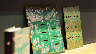
- Panel utilization: Collaborating with suppliers to optimize delivery panel layouts and sizes and to minimize material waste through efficient panelization strategies can significantly reduce production costs and environmental impact.
- Process capabilities: Aligning design requirements with the manufacturer’s process capabilities – including available equipment, feature size limitations, and certifications – ensures seamless production and compliance with industry standards.
- Testing and validation: Defining appropriate test protocols and integrating them into the manufacturing workflow helps identify and address potential issues early on, reducing the need for costly reworking or instances of field failures.
- Supply chain optimization: Streamlining the supply chain through standardization, modular assemblies, and careful connector selections can minimize lead times, inventory costs, and assembly complexities.
Successful DFM implementation requires a mindset within your organization that prioritizes collaboration with suppliers, continuous improvement, and a deep understanding of manufacturing constraints and opportunities.
Empower cross-functional teams
By empowering cross-functional teams, investing in DFM training, and leveraging the expertise of trusted partners, companies can unlock their full potential, allowing them to secure high-quality PCBs with optimized costs and a shorter time to market.

The copperdot DFM service
At Bosch, we leverage our DFM PCB expertise to offer material consultations and combinations that are critical for achieving high-performance end products. Drawing on our extensive experience with Bosch products, we understand the importance of choosing the right materials that meet the stringent requirements of your electronic projects. This specialized knowledge allows us to tackle complex challenges related to thermal management, electrical performance, and environmental considerations, ensuring that every PCB design is optimized for both manufacturability and end-user satisfaction.

Additionally, our engineers possess in-depth knowledge of the PCB manufacturing process and can provide valuable support along with their expertise. They offer fresh perspectives on your design, advise you on how to streamline your products, share concerns about quality, and assess whether your designs meet the latest PCB standards. They also provide feasibility studies for your projects, recommendations on material selection, insights into material performance, and much more.
Our team will be happy to advise you on any of the aforementioned topics and share our knowledge and expertise to ensure functionality, usability, and reliability combined with efficient and stable manufacturability.


